2D materials
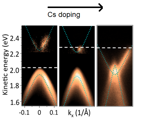
The present study concerns the monitoring by FemtoARPES of the evolution of the band structure of BP during the deposition of a thin layer of caesium or potassium. Such an alkaline layer induces the presence of a strong electric dipole on the surface which can modify the electronic structure of BP. The technique allows to observe the dispersion curves of the electronic states and to measure the gap with high accuracy. It can be noted that the relatively low energy of the probe beam gives a sufficiently long escape length to the excited electrons to reliably observe the evolution of the buried valence band. It is thus observed that during alkali deposition (i.e. by increasing the electronic doping) the gap monotonously narrows from the initial value of 0,32 eV for the bare sample, to zero for the largest cesium deposits. Moreover the figures shows that the "Fermi velocity" of the electrons becomes very high. In the high doping regime, the holes moving in the highly dispersive direction acquire a band velocity even higher than that of graphene on silicon carbide. This study shows that the electronic structure of black phosphorus can be easily shaped by electron doping. This engineering of the electronic band structure would enable the design of devices with improved and optimized electronic and optoelectronic functionality.

[1] Band Gap Renormalization, Carrier Multiplication, and Stark Broadening in Photoexcited Black Phosphorus, Zhesheng Chen, Jingwei Dong, Evangelos Papalazarou, Marino Marsi, Christine Giorgetti,Zailan Zhang, Bingbing Tian, Jean-Pascal Rueff, Amina Taleb-Ibrahimi, and Luca Perfetti, Nano Letters 19, 488 (2019).
[2] Spectroscopy of buried states in black phosphorous with surface doping, Zhesheng Chen, Jingwei Dong, Christine Giorgetti, Evangelos Papalazarou, Marino Marsi, Zailan Zhang, Bingbing Tian, Qingwei Ma, Yingchun Cheng, Jean-Pascal Rueff, Armina Taleb-Ibrahimi, Luca Perfetti, 2D Materials 7, 035027 (2020).


